CE263 electronic engineering
1. Introduction
The oscillator is a fundamental component within many electronic systems, principally as a source of timing (clock) information as in most complex digital systems, or to provide a continuous sinewave at a precisely controlled frequency. A high frequency sinewave oscillator is an essential component in, for example, a superhet radio receiver where the radio frequency (RF) signals from the antenna over a range of frequencies are converted to a convenient fixed 'Intermediate' frequency (IF) for channel selection, amplification and demodulation. The local oscillator runs at a frequency higher or lower than the signal from the antenna. Multiplying the two components together generates sum and difference frequencies, one of which, usually the difference, is the IF. To 'tune' the receiver, the local oscillator frequency has to vary in step with other frequency-selective circuits that track the incoming RF. This is very much easier to implement than doing all the signal processing at RF, particularly for frequencies above 30 MHz or so.
In this experiment we simulate and construct low (audio) frequency sinewave oscillators based on RC filters and operational amplifiers. We investigate how to ensure that the output waveform really is a pure sinewave: this turns out to require a feedback loop in addition to the one that ensures the oscillation. An important application for fully-analogue audio oscillators is the generation of a harmonic-free output that can be used to test high-quality audio amplifiers; a common performance criterion is the amount of harmonic distortion introduced by the amplifier. Obviously the test signal being used must be as 'clean' as possible to have confidence in the result.
Wein-Bridge oscillator
Fig. 1a shows the basic circuit of this well-known type of oscillator which comprises an operational amplifier with negative feedback to control gain, and frequency-dependent positive feedback to select the oscillation frequency.
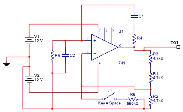
Figure 1a. Wein Bridge oscillator (circuit diagrams from Multisim).
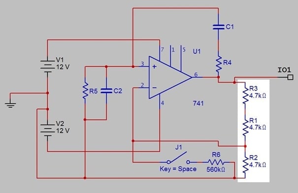
Figure 1b. Amplifier gain control components
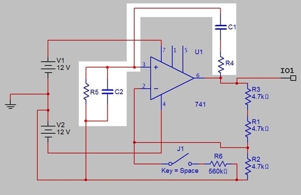
Figure 1c. Positive feedback frequency control components: 'lead-lag' network.
Fig. 1b highlights the gain control components. In this configuration, the voltage gain from the noninverting op amp input (pin 3) to its output (pin 6) is given by:
(R3+ R1)
Av=1+ R2
Fig. 1c shows the frequency control network, where the pairings of the components are not the obvious ones: C1, R5 have a 'phase lead' effect (differentiator), while C2, R4 cause 'phase lag' (integrator). Exact analysis is straightforward (Floyd, Appendix 1), but it is also easy to work out intuitively what the network will do, and how its output connected to pin 3 will vary with frequency.
At very low frequencies the reactances of C1 and C2 will be high, and the series combination C1, R5 will dominate. Current 'through' a capacitor is greatest when the rate of change of voltage across it is maximum; assuming a sinewave, this means the voltage across R5 has a phase shift (lead) approaching +90 degrees. The voltage amplitude will be small. This circuit approximates a differentiator.
At very high frequencies, the capacitor reactances are both low, and the combination R4, C2 dominates. For a sinewave again, current into C2 is at a maximum when voltage on R4 is maximum, so the voltage across C2 is maximum when voltage on R4 is zero. This gives the voltage across C2 a phase shift (lag) of -90 degrees. The voltage amplitude will again be small. This circuit approximates an integrator.
Hence as frequency increases from 'low' to 'high', phase shift varies between +90 and -90 degrees, and must at some stage pass through zero. At the same time, the voltage amplitude will have a maximum, at the zero phase shift frequency.
It can be shown that, if R5 = R4 and C1 = C2, then the maximum 'gain' from pin 6 to pin 3 of the op amp will be V3/ V6 = 1/3 at frequency fr, where:
f r= 2πRC1
More importantly for its use in the oscillator circuit, the phase shift, V6 to V3, at this frequency, will be zero. For proofs, see Floyd, Chapter 16, Equations 16-1 and 16-2, which are derived in Appendix 1B.
Experiment 1
Assuming R5 = R4 = 10 kΩ, calculate a value for C1 = C2 that will make the oscillation frequency 1 kHz, then select the nearest available value from the component drawers in the laboratory and recalculate the expected frequency. To save time, an instrumented Multisim 'template' of Fig. 1 has been attached in the folder, but note that C1 and C2 are placeholders with incorrect and hence non-functional values which have to be calculated.
In the hardware implementation, perform a quick frequency response check on the components highlighted in Fig. 1c, without the op amp in circuit and using a sinewave signal generator connected to R4. Examine the waveform amplitude and phase at the junction of C1 and C2 relative to the input sinewave, noting carefully the frequency and amplitude at which the phase shift is zero; note also how the phase varies for small changes of frequency each side of the zero-phase value.
Compare with your calculated values. (Using 'averaging' mode available via the oscilloscope Acquire menu will give best results.)
Measuring phase shift can be done from the oscilloscope traces by first finding the time delay between zero crossings of the two waveforms (use the cursor facility to locate them on-screen), then expressing this as a fraction of the period of oscillation. Multiplying by 360 gives the answer in degrees.
Experiment 2
After replacing C1 and C2 with your calculated value, activate the Multisim circuit of Fig. 1a. The amplifier gain is already designed to be +3, to ensure the loop gain is 1, one of the conditions for oscillation given the minimum attenuation of the lead-lag network. The components J1 (a switch) and R6 are designed to enable the loop gain to be raised slightly above 3 (you may need to experiment with the value of R6). Run the simulation first with J1 OPEN, i.e. R6 disconnected: it's likely nothing will happen. Close J1 for a second or so at a time with the simulation still running and note what happens. (Note that when the oscillation amplitude rises to maximum the simulator will probably 'crash'. Why is this?)
Experiment 3
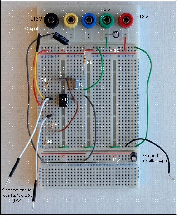
Construct a hardware version of Fig. 1. Remember to include decoupling capacitors (≈10 µF) from each power rail to ground. Replace the combination R1, R3 with an external resistance box. With the circuit under power, increase the resistance slowly (i.e. increase the loop gain) until you get oscillation – with the box you can do this very precisely and in small steps. Record its frequency. If the circuit oscillates at all, you should find that it is difficult to get an undistorted steady sinewave: the amplitude will either slowly die back to zero, or increase until it is limited by the power supplies, by which time it will no longer be sinusoidal and the frequency may not be close to its design value.
Adjust the loop gain for the best-looking stable sinewave you can get, and check its spectrum using the FFT function under Math on the oscilloscope. Ask a demonstrator if you are not familiar with this procedure, or need help to interpret the results. You may find that spectra are of better quality on the older Tektronix TDS210 instruments: see Tony de Roy to get one, and for advice on how to capture screen images from it.
Experiment 4
In the hardware of Experiment 3, adjust the variable resistor until the circuit just oscillates. Now break the positive feedback loop at a convenient point, and inject a signal from a signal generator into the appropriate side of the break. Compare the signal generator waveform with the output on the other side of the break at the oscillation frequency noted earlier. Do you get the expected results? How do the signals change as the signal generator frequency is varied slightly?
5. Amplitude Stabilisation
You should have noticed in previous experiments (if not in the Multisim simulation) that it is very difficult to fix the oscillation amplitude at a value that does not grow until limited by the power supply voltages, or decay to zero. In fact, in the hardware implementation it is impossible. The process is an example of unstable equilibrium, analogous to balancing a cone on its tip: in theory this can be done, but the slightest perturbation causes it eventually to lose balance and fall over.
The only way to ensure stability in the oscillator is to introduce another negative feedback loop where the amplifier gain is controlled by a signal proportional to the output: if the output increases above a set level, the gain must decrease, and vice versa. Floyd suggests one way of doing this which is to use a field effect transistor as a variable resistance where the resistance forms part of the gain control network round the op amp. We investigate a different method, based on a light dependent resistor, LDR. LDRs are commonly used as low-cost light sensors, for example to switch-on street lights around sunset.
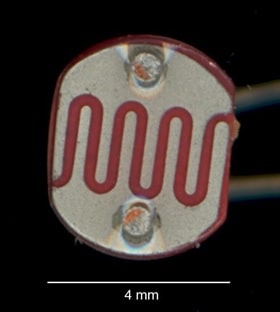
Figure 2. Light Dependent Resistor
Fig. 2 shows the device to be used in the experiment. It comprises a layer of semiconductor material, here cadmium sulphide (CdS), deposited on a ceramic substrate. CdS is very sensitive to light. Two interdigital[1] metallic contacts overlay the active material, which can be exposed to light in the gap. The controlling light source is an ordinary LED, placed close to the LDR (Fig. 3), both normally enclosed in a light-proof housing. This is an example of an opto isolator, devices used when systems need to communicate but cannot be directly connected electrically for safety reasons, for example if one part is running at high voltage. They are also used in as low-noise gain control devices in high-quality analogue audio systems. In our case, the LDR resistance will controlled by the LED current, such that as the current increases the resistance falls. The (very sparse) LDR datasheet is included in the Appendix 1.
[1] Like interlocking fingers.

Figure 3. Green light emitting diode and light dependent resistor mounted in silicone tube (above) and sealed in lightproof 'shrinkfit' (below). Using a green LED should match the peak sensitivity of the LDR material, which is to wavelength 540 nm. However, the photoresistor turns out to be very much more sensitive to light from a red LED, probably because these have greater overall light output. The devices in the laboratory use red LEDs.

Fig. 4a shows the typical electrical behaviour of the opto isolator devices used in the experiment: the ones you are using, shown in Fig. 3, have been assembled here. The lead with a piece of red sleeving is the anode of the LED. The LDR leads are unmarked as it is not polarised, behaving like a pure resistance. Fig.4b shows the resistance graph for a device using a red LED plotted on logarithmic axes. Note the high sensitivity to LED current change, and the very wide dynamic range of resistance. Be careful always to include a current-limiting resistor in series with the LED when testing and keep the maximum current below 20 mA.
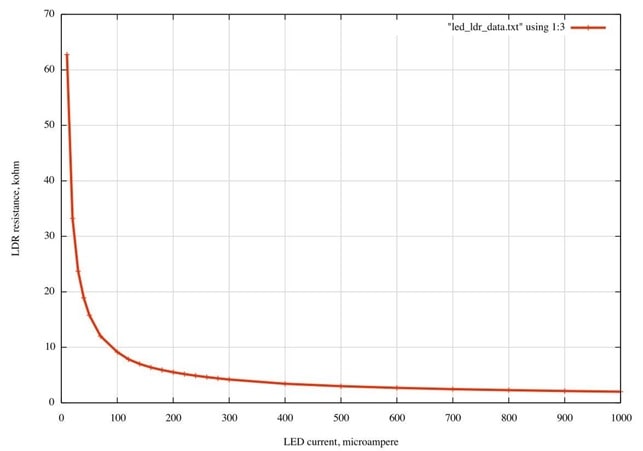
Figure 4a. LDR resistance, kΩ, as a function of LED current, µA. The light source for these measurements was a red LED.
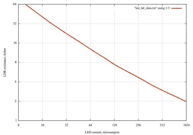
Figure 4b. Same as Fig. 4a, base 2 log axes.
Alternative method. Figure 4c shows the results of a direct determination of amplifier gain as a function of LED current: it uses more or less the circuit of Fig. 5b with the values of R1 and R2 shown, i.e. 33 kΩ and 4.7 kΩ. The positive feedback network and C3 are disconnected and the amplifier noninverting input fed directly from a signal generator. Also disconnect R7 and C5, and feed current directly to the anode of the LED. Output voltage for constant signal input is measured over a range of LED currents. What are the asymptotic values of the voltage gain if the LDR resistance is infinite (open circuit) or zero?
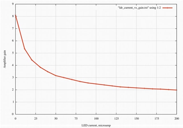
Figure 4c. Direct gain measurement as a function of LED current
Experiment 5
Measure the resistance characteristic of the opto isolator provided - you should vary the LED current over a range similar to that used above, i.e. up to about 1 mA maximum; the LED forwardbias voltage will be around 2 V, and only increase slightly with current. If you are not certain how to do this, ask a demonstrator. You will need this information later in the experiment – do not rely on the curves Fig. 4a-c as devices are likely to be quite variable one to the next.
Alternatively, use the method suggested for Fig. 4c, in which case the process can then be reduced to a single measurement, to find the LED current that makes the amplifier gain equal to 3. For the device tested (with a red LED) this came out at 64 µA.
6 Feedback Stabilised Oscillator
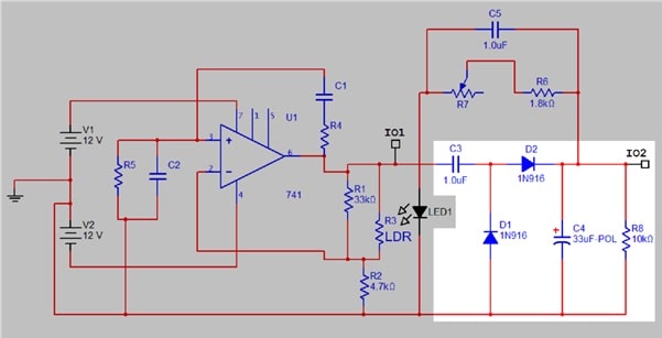
Figure 5a. Stabilised oscillator highlighting peak-peak rectifier
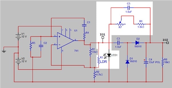
Figure 5b. Stabilised oscillator highlighting opto-isolator circuit
Figures 5a and b show the oscillator with the additional elements to stabilise its output amplitude. A peak-peak rectifier (5a) generates a smoothed positive DC level from the AC output of the oscillator. This is fed via a variable resistance (R7) to the LED half of the opto isolator, while the LDR replaces part of the gain control network in the oscillator itself. This acts in the correct sense: if output voltage (and hence the DC level) increases, LED current increases and the LDR resistance falls, hence reducing amplifier gain. The function of C5 is discussed further in Experiment 8.
Experiment 6
Build and test, or simulate, the highlighted part of Fig. 5a. Feed a 1 kHz sinewave from a signal generator into C3, using an amplitude range of 0 to 10 volts peak-peak. Record how the output DC level across C4 varies with the AC input signal, and explain your results. You should also explain how the circuit itself works, and why a common name for this configuration is a voltage doubler.[1]
Experiment 7
Based on the results from Experiments 5 it should be possible to work out the approximate current needed through the opto isolator LED to ensure stable oscillation, where the required LDR resistance is going to be that which makes the amplifier gain equal to 3. The method for Fig. 4c is the easiest for this.
Now, assume the output signal amplitude is to be some convenient level, say 3 V peak: this gives a value for the combined resistance of R6 and R7 (remember to take into account the LED forward bias voltage). Try inserting this value into the circuit and test it. Remember to include C5. Note that this can not be simulated in Multisim: as far as is known, an equivalent of the LED/LDR combination is not available in the component set.
Replace the fixed resistance R7 with a multiturn variable potentiometer, say 20 kΩ, which should give continuous control of the output signal amplitude.
Experiment 8
With the oscillator of Experiment 7 working normally, try removing C5 and observe what happens. You should find that the output signal amplitude varies between very large (limiting) and very small (near zero) voltages. The period of variation will be large relative to the oscillation period. This is a common effect in feedback control systems[2] and normally occurs when there is a degree of lag or delay in the control response; the lag in this case is mainly due to the charge/discharge characteristics of the DC smoothing circuit (C4/R8). Theoretical analysis is beyond the scope of the present work, and difficult anyway because of the nonlinear behaviour of the opto isolator. However, try and find a qualitative explanation of why the introduction of C5 is able to stabilise the amplitude control loop.
Experiment 9
Investigate the 'spectral purity' of the amplitude-stabilised oscillator, and compare with your results from Experiment 3. You may find that results are improved by inserting a unity gain buffer (an op amp with output connected to its inverting input) in the feed to the voltage doubler circuit. Why is this?
Experiment 10
Return to the circuit used in Experiment 3, and set R1+R3 so that the circuit does not oscillate (get it to oscillate, then adjust the resistance box so that oscillation just stops. The amplifier gain will be slightly less than 3). Now inject a sinewave signal from a signal generator into the amplifier
'virtual earth' summing point (op amp inverting input, pin 2) via a 10 kΩ resistor. Measure the frequency response of the output signal for a range of frequencies that includes the designed oscillation frequency and compare with the response you obtained from the passive CR network by itself in Experiment 1. Explain what you see. Hint: look up Active Filters.
Experiment 11
Investigate the performance of the oscillator as a variable frequency source: this will need a dual potentiometer so that R4 and R5 (Fig. 1a) can be varied together. See Tony de Roy.
[2] It is possible to cascade circuit elements like this to produce very high DC voltages at low current, as in the CockcroftWalton Multiplier.
Appendix 1
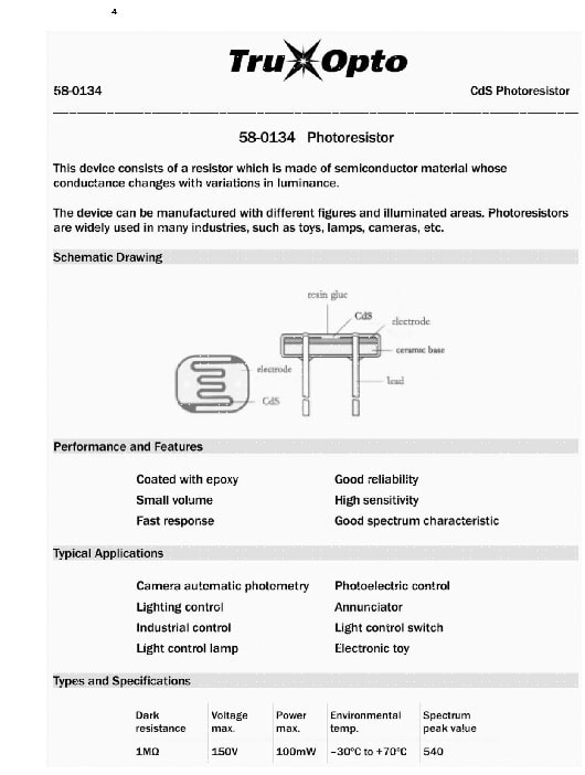
Datasheet
4 Source: Rapid Electronics Ltd.
741 electrical connections (top view of IC)
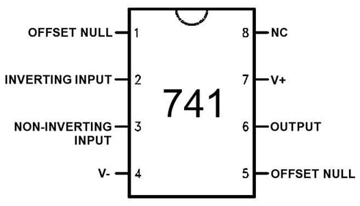
OFFSET NULL and NC (no connection) inputs can be ignored. For a full datasheet, see for example:
http://www.ti.com/general/docs/lit/getliterature.tsp?
genericPartNumber=lm741®=en&fileType=pdf Appendix 2 – typical breadboard layout for the basic oscillator.
