

When the output the memory element logical
| 566 | C H A P T E R |
|
CM | RL | |||
|---|---|---|---|---|---|---|---|
| dIN | * | ||||||
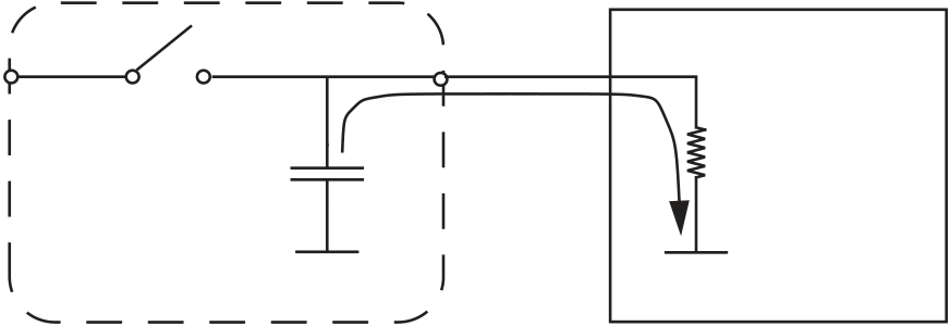
| FIGURE 10.58 Memory | |||||||
| Store = 0 | |||||||
| capacitor discharge due to load | |||||||
| resistances for the unbuffered | Memory element | dOUT | |||||
| memory element. | |||||||
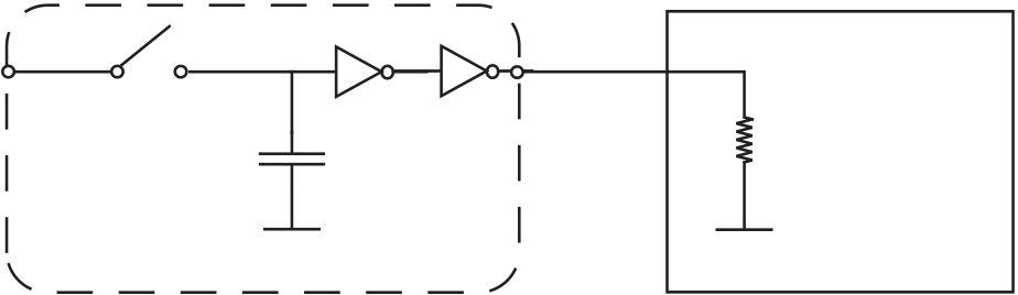
| FIGURE 10.59 Memory | dIN | * | RL | ||||
| Store = 0 | |||||||
| CM | |||||||
| capacitor’s charge is protected in | |||||||
the buffered memory element.
Memory element External logic device
| FIGURE 10.60 Charge leakage | dIN |
|
* |
|
dOUT | |
|---|---|---|---|---|---|---|
| from the memory capacitor for the | ||||||
| buffered memory element. |
| 10.7 Digital Memory | 567 |
|---|
see Equation 10.26). When a capacitor CM charged to an initial voltage VS discharges through a resistor RP, its voltage vC as a function of time is given by the following equation:
vC = VSe−t/RPCM.
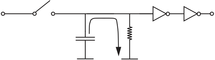
The one-bit memory element that we have discussed thus far is called a dynamic one-bit memory element or a dynamic D-latch. It is dynamic in the sense that it stores a value written into it only for a finite amount of time (due to nonzero parasitic resistances in practical implementations). The static one-bit memory element or a static D-latch is another type of memory element that has the same logic properties as the dynamic D-latch, but can store a value written into it indefinitely.
Figure 10.61 shows one possible circuit for a static memory element. In this circuit, a non-ideal switch with a very high ON resistance is connected between the power supply and the storage node of the memory element. When the output of the memory element is a logical 1, this switch is turned on and introduces a small stream of charge into the storage node to offset any leakage. Because it trickles charges into the node, this switch is called a trickle switch. The ON resistance of the trickle switch is made very large compared to the ON resistance of the store switch, so that the trickle input can be overridden easily by the input dIN. A detailed circuit design of the static latch is beyond the scope of this book. The interested reader is referred to ‘Principles of CMOS VLSI Design,’ by Weste and Eshraghian.
| dIN | * | dOUT | FIGURE 10.61 Circuit |
|---|---|---|---|
CM


