

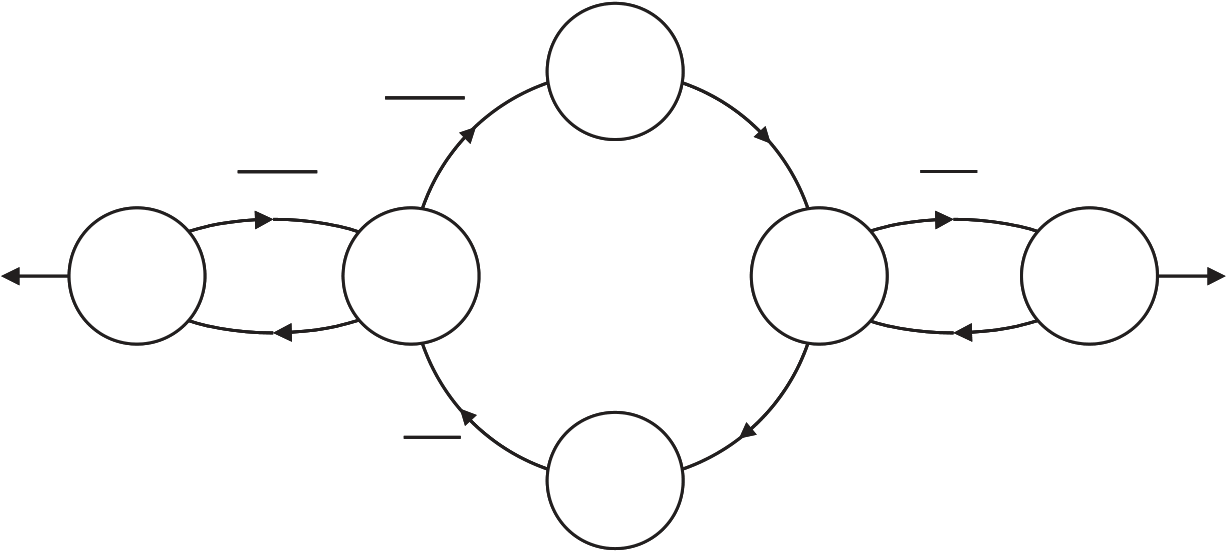
The state transition diagram such circuit shown fig
| Design of High Power Class-D Audio Amplifiers | 30 |
|
225 | ||
|---|---|---|---|---|---|
| 30 | VP,VM [V] | ||||
|
20 | 40 | (a) |
|
80 | time[∝s] | VLOAD | 400 | sticking | 800 | time[∝s] | ||
|---|---|---|---|---|---|---|---|---|---|---|---|---|---|
| 200 | (b) |
The clipping recovery behavior can be improved significantly if the integrators are prevented from diverging during clipping. To do so the onset of clipping needs to be detected and corrective action needs to be taken to keep the integrators near their steady-state values.
Detection of clipping in the class-D feedback loop is fairly simple. As can be seen in Fig. 10, during normal operation a fixed sequence exists in the transitions of the reference clock signal osc and the comparator output signal pwm. A rising edge of the osc signal is always followed by a rising edge of the pwm signal and a falling edge of the osc signal is always followed by a falling edge of the pwm signal. A deviation from this sequence can be detected by a simple asynchronous logic circuit. The state transition diagram of such a circuit is shown in Fig. 19.
| S3a | pwm | S0 | osc | osc | S1a | clip=1 | ||
|---|---|---|---|---|---|---|---|---|
| osc | S2 | S1 | pwm | |||||
| osc | pwm |
226 M. Berkhout
cycle can prevent this. For the first integrator this can be achieved by temporarily
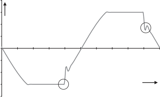
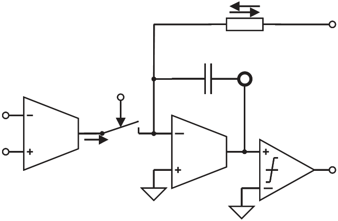
interrupting the current from the VI-converter gm0. This will automatically cause the output VP of the first integrator to change direction and return towards zero. After a comparator detects a zero crossing the current from VI-converter gm0 is resumed. This system is shown schematically in Fig. 20. Note that a comparator to
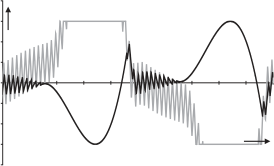
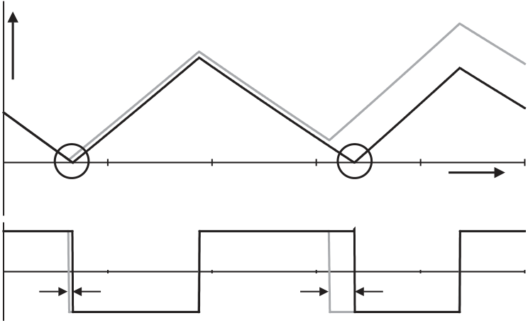
edges the osc signal. As can be seen in Fig. 21 the negative peaks of triangular wave VM stop crossing zero when positive clipping starts. A zero crossing can be forced when the edge of the osc signal is delayed. As can be seen in Fig. 21, this causes
IPWM
| Fig. 20 Forcing zero crossing of first integrator | VIN | g m0 | I IN | C1 | V P | sign1 | ||
|---|---|---|---|---|---|---|---|---|
| S1 | g m1 |
VM
| Fig. 21 Integrator output VM and
osc with and without edge delay |
osc |
|
time |
|---|---|---|---|
| edge delay |


