Sinusoidal waveform the reference signal
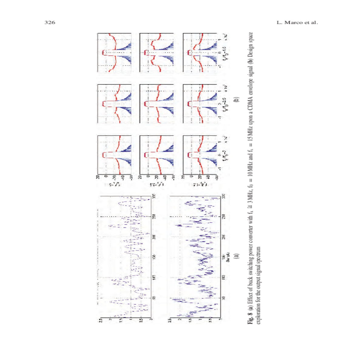
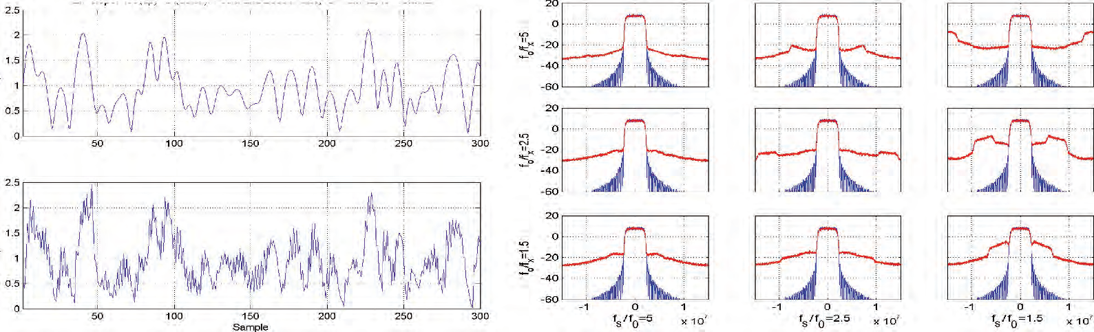
| 326 | (b) | Fig. 8 (a) Effect of buck switching power converter with fx ∼= 3 MHz, f0 = 10 MHz and fs = 15 MHz upon a CDMA envelope signal (b) Design space exploration for the output signal spectrum |
|
|
|---|---|---|---|---|
| (a) |
| Wideband Efficient Amplifiers for On-Chip Adaptive Power Management Applications | VC | 327 | ||||||||||||||||||
|---|---|---|---|---|---|---|---|---|---|---|---|---|---|---|---|---|---|---|---|---|
| Q1 | Q3 | g4 | L3L | + | g1 |
|
VC | Vin-VC | VC | |||||||||||
| g3 | ||||||||||||||||||||
| g1 | g3 | Q4 | VSW | Vin | ||||||||||||||||
| Vout | ||||||||||||||||||||
| (D < 0.5) | Vin/2 | |||||||||||||||||||
| Cx | ||||||||||||||||||||
| Vin | g2 | Q2 | R | g1 | Vin | |||||||||||||||
| _V C | ||||||||||||||||||||
| _ | ||||||||||||||||||||
| g3 | ||||||||||||||||||||
| VSW | VC | Vin | Vin-VC | Vin | VC | Vin | Vin-VC | Vin | ||||||||||||
| Vin /2 | ||||||||||||||||||||
| (D > 0.5) | ||||||||||||||||||||
| 0 | Ts/2 |
|
t | |||||||||||||||||
| (a) | (b) | |||||||||||||||||||
1 V three level buck 1.0V three level buck
0.5 V
| 0 V 1 V | 200 ms | 250 ms | ||||
|---|---|---|---|---|---|---|
3.0 mV
|
||||||
| 0.5 V | ||||||
| 0 V | 100 ms | |||||