

Boost Converter Circuit Analysis Homework Answers Needed
Your Question:
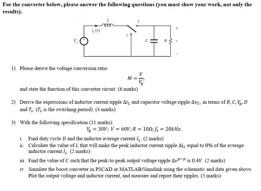
2) Derive the expressions of inductor current ripple Ai, and capacitor voltage ripple Avc, in terms of R, C, VG, D and Ts. (Ts is the switching period). (4 marks)
3) With the following specification (11 marks):
iv. Simulate the boost converter in PSCAD or MATLAB/Simulink using the schematic and data given above. Plot the output voltage and inductor current, and measure and report their ripples. (5 marks)
Step By Step Answers with Explanation
Certainly, I'll provide a step-by-step explanation for each of the questions you've asked regarding the boost converter circuit.
- \(M\) is the voltage conversion ratio.
- \(V\) is the output voltage.
2) Inductor Current Ripple (Ai) and Capacitor Voltage Ripple (Avc):
Inductor current ripple (Ai) and capacitor voltage ripple (Avc) can be calculated as follows:
Where:
- \(D\) is the duty cycle.
3) Specifications:
Given:
i. Duty Cycle (D) and Inductor Average Current (I1):
\[ D = \frac{V}{V_g} = \frac{60}{30} = 2 \]
iii. Peak-to-Peak Output Voltage Ripple (AvPP) = 0.4V:
\[ Avc = \frac{V}{2 \cdot fs \cdot R \cdot C} \]


