
Illustrated the mosfet schematic figure
| 12.17 Capacitance | ● | S-99 |
|---|
typically on the order of 6 mm (�� in.) on a side and contains thousands of circuit elements: diodes, transistors, resistors, and capacitors. One such micropro-cessor chip is shown in its entirety in Figure 20.22b; also shown are the numerous electrical leads that are used to connect this chip to its leadframe, which in turn is bonded to a printed circuit board. Enlarged photographs of microprocessor chips at different magnifications are presented in Figures 12.25a and 12.25b; these micrographs reveal the intricacy of integrated circuits. At this time, 175,000,000 component chips are being produced, and memory capabilities cur-rently double about every 12 months.
Microelectronic circuits consist of many layers that lie within or are stacked on top of the silicon wafer in a precisely detailed pattern. Using photolithographic techniques, for each layer, very small elements are masked in accordance with a microscopic pattern. Circuit elements are constructed by the selective introduction of specific materials (by diffusion or ion implantation) into unmasked regions to create localized n-type, p-type, high-resistivity, or conductive areas. This procedure is repeated layer by layer until the total integrated circuit has been fabricated, as illustrated in the MOSFET schematic (Figure 12.24). Elements of integrated circuits are shown in Figure 12.25 and in the chapter-opening photograph for this chapter.
|
(12.27) |
|---|
where V is the voltage applied across the capacitor. The units of capacitance are coulombs per volt, or farads (F).
| C � �0A l | (12.28) |
|---|
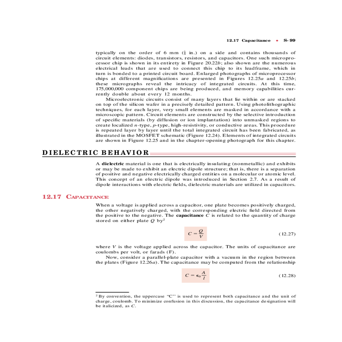
| ● | Chapter 12 / Electrical Properties | E | = | V |
|
V | |||
|---|---|---|---|---|---|---|---|---|---|
|
|||||||||
| D0 = �0E | |||||||||
|
|||||||||
|
|||||||||
| l | |||||||||
| l | |||||||||
|
|||||||||
|
|||||||||
| Dielectric | P |
|---|
(b)
where A represents the area of the plates and l is the distance between them. The parameter �0, called the permittivity of a vacuum, is a universal constant having the value of 8.85 � 10�12F/m.
| (12.29) |
|---|
| (12.30) |
|---|
which is greater than unity and represents the increase in charge storing capacity by insertion of the dielectric medium between the plates. The dielectric constant is one material property that is of prime consideration for capacitor design. The �r values of a number of dielectric materials are contained in Table 12.4.


