
Half mode substrate integrated waveguide hmsiw
Half Mode Substrate Integrated Waveguide (HMSIW) Loaded Evanescent-Mode Bandpass Filter
I.Introduction
Microwave filters are integral components in systems for wireless
communication, audio and video broadcast, radar, power transmission,
imaging, and sensors. Design and miniaturization of microwave filters is
an ongoing research topic where filters are designed for specified
performance such as bandwidth, insertion loss, and spurious-free range,
while minimizing size, weight, and cost.
High-performance narrow-band fabrication microwave filters have
traditionally been implemented in air-filled waveguide form with
attendant large size, high weight, and costly fabrication [1]. Waveguide
structures have been fabricated in planar form using printed circuit
board (PCB) manufacturing processes to form dielectric-loaded substrate
integrated waveguides (SIW) that reduce size, maintain waveguide
performance, and are as easily fabricated as planar microwave filters
[2].
This paper is organized as follows: Section II presents the design of third-order filters in evanescent-mode SIW and HMSIW form. Section III presents simulation model and measured filter S-parameter results, and compares filter size with conventional SIW resonators. Section IV summarizes the work and conclusions.
II.Filter Design
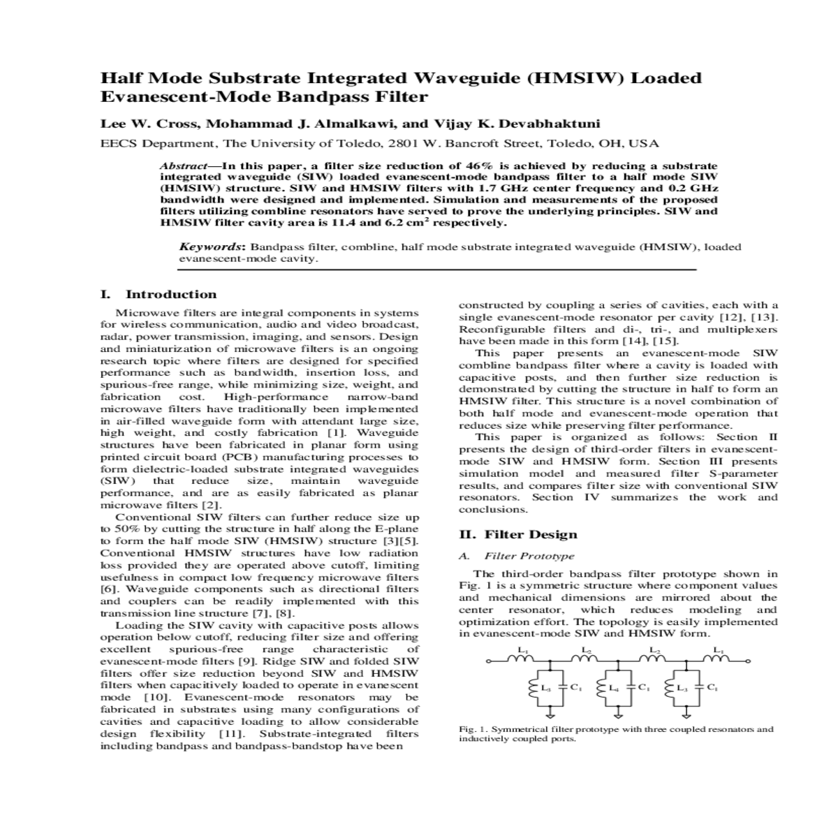
Fig. 1. Symmetrical filter prototype with three coupled resonators and inductively coupled ports.
| Description |
|
HMSIW Value | |
|---|---|---|---|
| C1 | Resonator capacitance | 16.93 pF | 8.47 pF |
| L1 | Port coupling | 3 nH | 6.2 nH |
| L2 | Inter-resonator coupling | 6.8 nH | 13.5 nH |
| L3 | Outer resonator inductance | 0.591 nH | 1.261 nH |
| L4 | Inner resonator inductance | 0.608 nH | 1.217 nH |
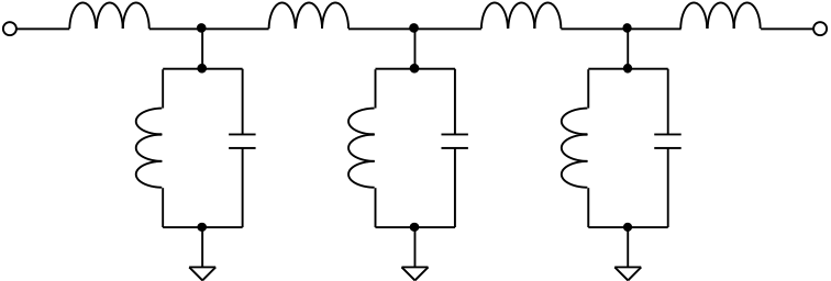
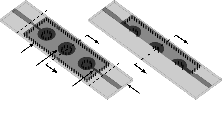
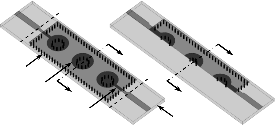
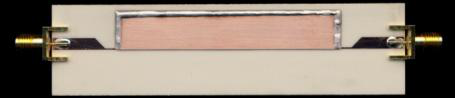
B.Physical Structure
cavity cut in half along the E-plane (feed line) axis, exposing the centerline of the cavity and posts. Edges of the feed and matching lines are aligned with the centerline. In this way filter area is reduced by half. Parameters of the HMSIW filter are adjusted to achieve identical filter performance.
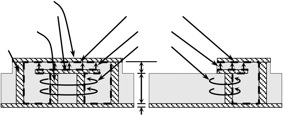
E-field at capacitive hats is shown by vertical vectors in Fig. 2 sections. H-field around resonator posts is shown with horizontal circular vectors. Current flows at the surface of the conductors inside the cavity along the path defined by the dashed lines.
The HMSIW filter requires smaller post radii R1 and R2 to maintain equal center frequency. Weaker port and inter-resonator coupling are realized with higher impedance matching lines (reduced Mw) and longer inter-resonator spacing, S.
|
0.85 | L | 24 | |||||||
|---|---|---|---|---|---|---|---|---|---|---|
| Mw | ||||||||||
|
||||||||||
|
3.35 | W | ||||||||
| B | ||||||||||
| 2X port matching | substrate | Ø0.7 | 3X øD | R2 | 2X R1 | |||||
| (a) | (b) | |||||||||
| (a) | ||||||||||
| L | ||||||||||
|
||||||||||
|
Mw | S | W | |||||||
| tlid | Ml | 3X øD | 2X R1 | |||||||
| tsub | ||||||||||
| 100 | ||||||||||
| tcu | (b) | |||||||||
| SECTION A | SECTION B |
|
||||||||
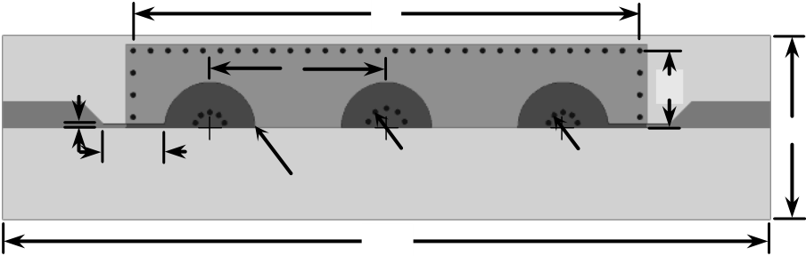
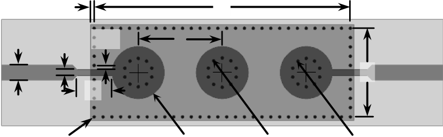
Fig. 2. (a) SIW and (b) HMSIW filter implementations showing cavity
structure, port matching lines, and resonators integrated into substrate.
| C | ε | 0 | 2 |
(1) | ||
|---|---|---|---|---|---|---|
| 1 | t | |||||
| Description |
|
HMSIW Value (mm) |
|
|---|---|---|---|
| L | Cavity length | 57.20 | 62.20 |
|
|---|
(c) |
|---|
| W | 20.00 |
|
0 |
|
1.4 | 1.5 | 1.6 | 2.0 | ||||||
|---|---|---|---|---|---|---|---|---|---|---|---|---|---|---|
| S | Resonator spacing | 18.60 | ||||||||||||
| R1 | Outer post radius | 2.82 |
|
|||||||||||
| R2 | Inner post radius | 2.90 |
|
-10 | 2.1 | 2.2 | ||||||||
| Mw | Matching line width | 2.50 | ||||||||||||
| Ml | Matching line length | 8.00 | ||||||||||||
| D | Post hat diameter | 11.80 | ||||||||||||
| tlid | Lid layer thickness | 0.203 | ||||||||||||
| tsub | 1.524 | |||||||||||||
| -30 | ||||||||||||||
| tcu | Copper thickness | 0.035 | ||||||||||||
| -40 | ||||||||||||||
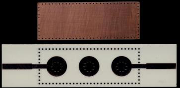
| standard two-layer PCB processing and impedance | ||||||||||||||
| control for ±10% transmission line tolerance. Lid layers | 0 | |||||||||||||
|
||||||||||||||
| were fabricated from single-sided laminate and attached | ||||||||||||||
|
||||||||||||||
| to substrates with short wires soldered through each via | ||||||||||||||
| barrel connecting top and bottom. Filters use SMA edge | -10 | |||||||||||||
| connectors. | ||||||||||||||
-30
| -40 |
|
1.4 | 1.5 | 1.6 | 2.0 | 2.1 | 2.2 | |
|---|---|---|---|---|---|---|---|---|
parameters for (a) proposed SIW; and (b) HMSIW filters.
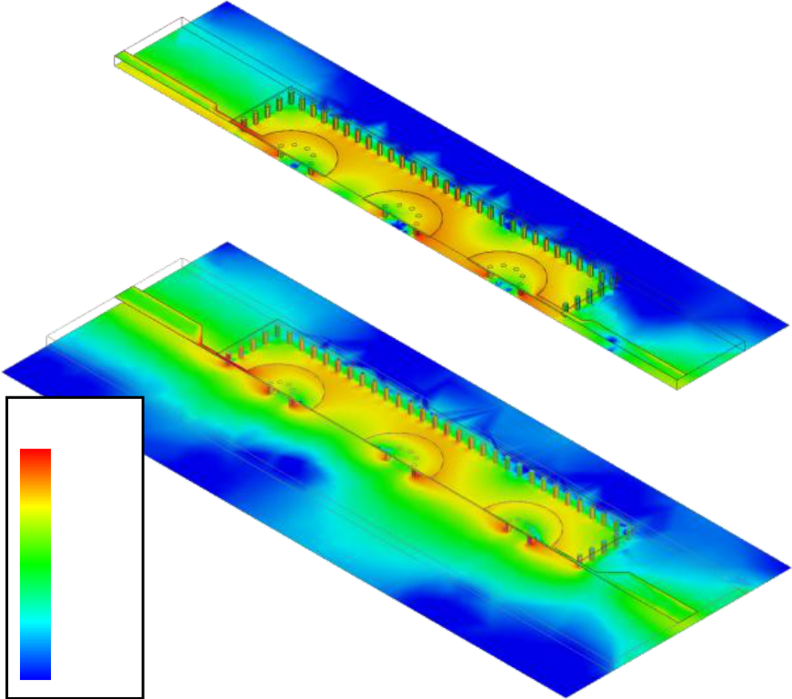
| Surface current density is shown in Fig. 6 for both filters. Current on the cavity top is not shown and the lid and substrate are transparent to see within the cavity structure. The SIW filter in Fig. 6(a) is sectioned along the center of the feed line to show current crowding at the base of the posts, which is also evident in the HMSIW filter in Fig. 6(b). Current is effectively contained within the cavity walls, although the HMSIW cavity opening allows some current outside the cavity. | ||
|---|---|---|
|
||
|
||
| -70 | Simulated |
|---|
| (a) | -80 | 2 | 3 |
|
7 | 8 | ||
|---|---|---|---|---|---|---|---|---|
| 0 | (a) |
| (b) |
|
|||
|---|---|---|---|---|
|
||||
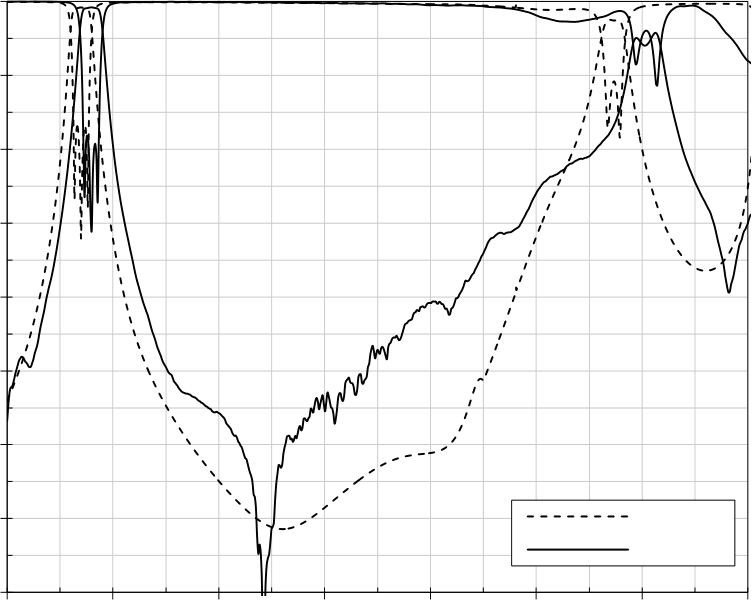
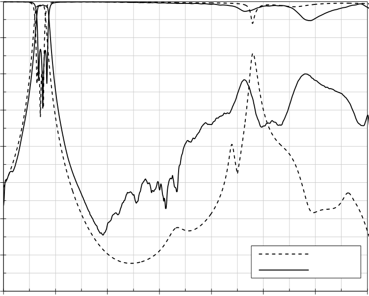
The wide-band responses in Fig. 7 show spurious-free performance to at least 6.5 GHz for SIW filters and beyond 8 GHz for HMSIW. Spurious response frequency can be increased further by reducing the substrate dielectric constant or reducing capacitive hat diameter, both of which increase the filter resonant frequency and must be compensated by increasing cavity size or decreasing post radius.
A concern of cutting the cavity in half is radiating energy from the open structure. The broadband filter response shows similar evanescent-mode SIW and HMSIW performance, particularly with similar S21 traces up to the spurious response frequency range; meaning that significant energy is not radiated from the cavity relative to the SIW structure. Unlike a conventional HMSIW filter, energy is well contained by the evanescent-mode cavity structure where the passband center frequency is half the cavity cutoff frequency.
| -80 |
|
2 | 3 |
|
7 | 8 |
|---|
| f | c 10 |
2 W |
(2) |
|---|
| f | r | 2 | c | 1 | 2 | 1 |
|
(3) | ||
|---|---|---|---|---|---|---|---|---|---|---|
| ε | W | L |
For a filter with center frequency of 1.7 GHz fabricated from a substrate with εr=3.55, similar to the proposed filters, each resonator can be 66 mm × 66 mm for minimum possible third-order filter area of 131 cm2. The first spurious passband, fr102, is calculated from (4) to be 2.7 GHz, which is much closer to the passband than with evanescent-mode SIW and HMSIW filters.
| f | r | 2 | c | 1 | 2 | 2 | (4) | |||
|---|---|---|---|---|---|---|---|---|---|---|
| ε | W | L |
Size reduction of evanescent-mode filters is significant versus waveguide filter implementation. The SIW evanescent-mode filter area is 11.4 cm2 versus the conventional SIW filter area of 131 cm2. The HMSIW filter area is 6.2 cm2 for a size reduction of 46% with similar S-parameters.
IV.Conclusions
[3]Y. Wang, W. Hong, Y. Dong, B. Lui, H. J. Tang, J. Chen, X.
Yin, K. Wu, “Half mode substrate integrated waveguide (HMSIW) Bandpass Filter,” IEEE Microwave Wireless Component Letters, vol. 17, no. 4, pp. 265-267, Apr. 2007.
[8]B. Liu, W. Hong, Y. Q. Wang, Q. H. Lai, K. Wu, “Half mode substrate integrated waveguide (HMSIW) 3-dB coupler,” IEEE Micro. Wireless Comp. Lett., vol. 17, no. 1, pp. 22-24, Jan. 2007. [9]R. W. Rhea, HF Filter Design and Computer Simulation, Norcross, GA: Noble Publishing Corp., pp. 363-371, 1994.
[10]L. S. Wu, X. L. Zhou, W. Y. Yin, “Evanescent-mode bandpass filters using folded and ridge substrate integrated waveguides (SIWs),” IEEE Microwave and Wireless Component Letters, vol. 19, no. 3, pp. 161-163, Mar. 2009.
[14]H. Sigmarsson, “Widely tunable, high-Q, evanescent-mode
cavity filters: Fabrication, control, and reconfigurability,” Ph.D.
Biographies
Lee Cross received B.S. and M.S. degrees in
summer of 2011, he was an intern with Freescale Semiconductor, Inc. working on modeling RF/Microwave components for the development of product-level models. He is a Postdoctoral Research Associate in the EECS Department at the University of Toledo. His current research interests include RF/Microwave circuit design and modeling, UWB antennas, and electromagnetic compatibility.
Vijay Devabhaktuni received the B.Eng. degree in
Toledo. Dr. Devabhaktuni’s R&D interests include applied electromagnetics, biomedical applications of wireless sensor networks, computer aided design, device modeling, image processing, infrastructure monitoring, neural networks, optimization methods, RF/microwave devices, and virtual reality applications. In these areas, he secured external funding close to $4M (sponsoring agencies include AFOSR, CFI, ODOT, NASA, NSERC, NSF, as well as industry). He co-authored 100 peer-reviewed papers, and is advising 17 MS/PhD students and 3 PDFs. He has won several teaching excellence awards in Canada and USA. Dr. Devabhaktuni currently serves as the Associate Editor of the International Journal of RF and Microwave Computer-Aided Engineering. He is a registered member of the Association of Professional Engineers, Geologists and Geophysicists of Alberta and is a Senior Member of the IEEE.


