

Figure shows the circuit schematic and differential logic gate
|
|---|
 |
|
|
||
|---|---|---|---|---|
|
|
|||
| E | ||||
Figure 6.67 Restructuring logic to enable implementation using non-inverting Domino Logic.
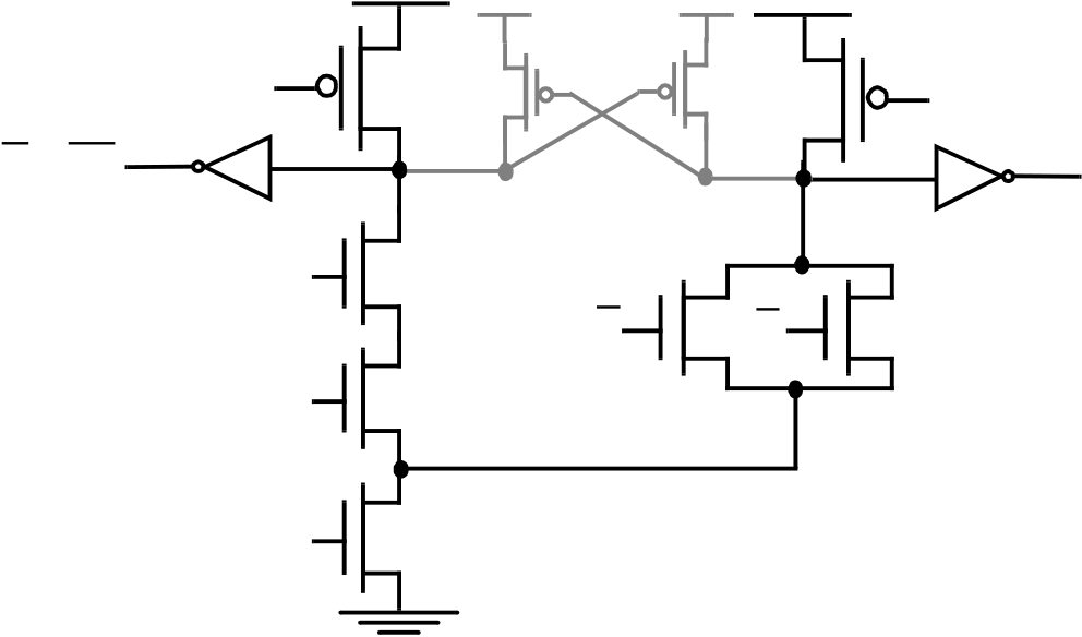
A general but expensive approach to solving the problem is the use of differential logic. Dual-rail Domino is similar in concept to the DCVSL structure discussed earlier, but uses a precharged load instead of a static cross-coupled PMOS load. Figure 6.68 shows the circuit schematic of an AND/NAND differential logic gate. Note that all inputs come from other differential Domino gates, and are low during the precharge phase, while making a conditional 0→1 transition during evaluation. Using differential Domino, it is possible to implement any arbitrary function. This comes at the expense of an increased power dissipation, since a transition is guaranteed every single clock cycle regardless of the input values—either O or O must make a 0→1 transition. The function of transistors Mf1 and Mf2 is to keep the circuit static when the clock is high for extended periods of time (bleeder). Notice that this circuit is not ratioed, even in the presence of the PMOS pull-up devices! Due to its high-performance, this differential approach is very popular, and is used in several commercial microprocessors.
A M1
A B
the transistors in the static inverter. With the inclusion of the evaluation devices in Dom-ino circuits, all gates precharge in parallel, and the precharge operation takes only two gate delays—charging the output of the dynamic gate to VDD, and driving the inverter out-put low. The critical path during evaluation goes through the pull-down path of the dynamic gate, and the PMOS pull-up transistor of the static inverter. Therefore, to speed up the circuit during evaluation, the beta ratio of the static inverter should be made high so that its switching threshold is close to VDD. This can be accomplished by using a small (minimum) sized NMOS and a large PMOS device. The minimum-sized NMOS only impacts the precharge time, which is limited in general due to the parallel precharging of all gates. The only disadvantage of using a large beta ratio is a reduction in noise margin. A designer should therefor simultaneously consider the reduced noise margin and perfor-mance during the device sizing.
Numerous variations of Domino VDD
logic have been proposed [Bernstein98].VDD to produce the correct results. Given
that the internal nodes precharge to VDD, the number of devices driving precharge devices is not reduced. However, the number of evaluation transistors is drastically reduced as they are amortized over multiple outputs. Additionally, this approach results in a reduction of the fan-out factor, once again due to the reuse of transistors over multiple functions.Compound Domino (Figure 6.70) represents another optimization of the generic Domino gate, once again minimizing the number of transistors. Instead of each dynamic gate driving a static inverter, it is possible to combine the outputs of multiple dynamic gates with the aid of a complex static CMOS gate, as shown in Figure 6.70. The outputs of three dynamic structures, implementing O1 = A BC, O2 = DEF and O3 = GH, are com-bined using a single complex CMOS static gate that implements O = (o1+o2) o3. The total logic function realized this way equals O = A B C D E F + GH.


