

Draw the diagram four-bit parallel adder utilising the symbol
3. LAB ACTIVITIES INTEGRATED CIRCUITS (IC) REQUIRED
74HC00 (Quad 2 input NAND gate), 74HC08 (Quad 2 input AND gate), 74HC32 (Quad 2 input OR gate), 74HC04 (Hex Not gates).
3.1.Pre-lab:
Given the truth table as below, write the Boolean expression for
output X in Sum-Of-Product (SOP) form.
| INPUTS | OUTPUT | ||
|---|---|---|---|
| A | X | ||
| 0 | 0 | 0 | |
| 0 | 0 |
|
0 |
| 0 | 1 |
|
0 |
| 0 | 1 | 1 | |
| 1 | 0 | 1 | |
| 1 | 0 | 1 | |
| 1 | 1 | 0 | |
| 1 | 1 |
|
1 |
1
f. Draw the implementation diagram of the simplified expression using relevant ICs. How many ICs are needed to implement this diagram?
2
| Message | Even parity bit | ||
|---|---|---|---|
| X | P | ||
| 0 | 0 |
|
|
| 0 | 0 |
|
|
| 0 | 1 | ||
| 0 | 1 | ||
| 1 | 0 | ||
| 1 | 0 | ||
| 1 | 1 |
|
|
| 1 | 1 |
|
|
Refer to Section 4.7 of the textbook (Parity Generator and Checker).
3
m.Fill in the truth table below for a parity checker using even parity. The parity checker produces an output Error bit E based on the 3 message bits (X, Y, Z) and the even parity bit P it receives. E=1 indicates error in the received data, and E=0 indicates no error.
| Message | Even parity bit | Error bit | ||
|---|---|---|---|---|
| X | P | E | ||
| 0 | 0 | 0 | 0 | |
| 0 | 0 | 0 | 1 | |
| 0 | 0 | 1 | 0 | |
| 0 | 0 | 1 | 1 | |
| 0 | 1 | 0 | 0 | |
| 0 | 1 | 0 | 1 | |
| 0 | 1 | 1 | 0 | |
| 0 | 1 | 1 | 1 | |
| 1 | 0 | 0 | 0 | |
| 1 | 0 | 0 | 1 | |
| 1 | 0 | 1 | 0 | |
| 1 | 0 | 1 | 1 | |
| 1 | 1 | 0 | 0 | |
| 1 | 1 | 0 | 1 | |
| 1 | 1 | 1 | 0 | |
| 1 | 1 | 1 | 1 | |
n. Fill in the K-map for the output Error bit E.
XY
o. Write the Boolean expression for the output Error bit
E. Represent the expression as XOR functions among the input
variables
Refer to Section 4.7 of the textbook (Parity Generator and
Checker).
r. Modify the design of the even parity generator in part 3.1l to odd parity generator. s.Modify the design of the even parity checker in part 3.1q to odd parity checker.
5
b. For the synchronous (parallel) counter shown in Figure 6, re-design the circuit indicated within the circle so that only two-input AND gates are used. Write down the necessary IC numbers and their pin numbers to implement this circuit.
6
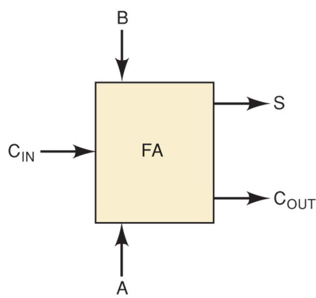
3.3.Pre-lab:
a. Fill in the truth table of the Full Adder (FA) below.
| A | B | CIN | S | COUT |
|---|---|---|---|---|
| 0 | 0 | 0 | ||
| 0 | 0 | 1 | ||
| 0 | 1 | 0 | ||
| 0 | 1 | 1 | ||
| 1 | 0 | 0 | ||
| 1 | 0 | 1 | ||
| 1 | 1 | 0 | ||
| 1 | 1 | 1 |
9
10
Table II. Segment values required to display hexadecimal digits 0‒F
| Segment | Hex value |
|---|---|
| Segment_a | 3812 |
| Segment_b | |
| Segment_c | |
| Segment_d | |
| Segment_e | |
| Segment_f | |
| Segment_g |
b. From the truth table, fill in the K-Maps for segments ‘a’ and ‘b’
c. From the K-Map, determine the minimised logic expression for ‘a’ and ‘b’
12


