Language:EN
Pages: 2
Rating : ⭐⭐⭐⭐⭐
Price: $10.99
Page 1 Preview
calculate the maximum input power

Calculate the maximum input power
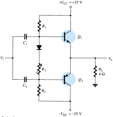
PL

pull operation is achieved by using complementary transistors (Q1 and Q2) before the matched npn output transistors (Q3 and Q4). Notice that transistors Q1 and Q3 form a Darlington connection that provides output from a low-impedance emitter-follower.

EXAMPLE 16.10

For the circuit of Fig. 16.19, calculate the input power, output power, and power handled by each output transistor and the circuit efficiency for an input of 12 V rms.

Figure 16.19

Vi(p) � �2� Vi (rms) � �2� (12 V) � 16.97 V � 17 V

Since the resulting voltage across the load is ideally the same as the input signal (the

Po(ac) � �2 R� � �

L 2 ( 4
� � 36.125 W

L
p) 1

4
7� � 4.25 A

Chapter 16

� � 2.71 A 5 A)

PL

PQ � �P 2 2Q� � �Pi

2
� �Po

% � � �P

P

.7 2� � 100% � 53.3% 5 5

W
W

EXAMPLE 16.11


V

R
� � �
2

� ) )
2

[Note that the maximum efficiency is achieved:]

P2QPiPo � 99.47 W � 78.125 W � 21.3 W

For the circuit of Fig. 16.19, determine the maximum power dissipated by the output transistors and the input voltage at which this occurs.

EXAMPLE 16.12

2R
� � �
2

L
2

VL � 0.636VL(p) � 0.636(25 V) � 15.9 V

(Notice that at VL � 15.9 V the circuit required the output transistors to dissipate 31.66 W, while at VL � 25 V they only had to dissipate 21.3 W.)

16.5
703

You are viewing 1/3rd of the document.Purchase the document to get full access instantly

Immediately available after payment
Both online and downloadable
No strings attached
How It Works
Login account
Login Your Account
Place in cart
Add to Cart
send in the money
Make payment
Document download
Download File
img

Uploaded by : Joshua Johnson

PageId: DOCB7926E5