

And test mux using and logictask task statement the task
Introduction
In this lab, the expected learning objective of this lab is to gain experience using LogicWorks to build and debug circuits and subcircuits that perform mathematical operations and route data.
Task 2-1: Work Preformed
For this task, I used the truth table for the full adder given in the lab manual to derive the SUM and Cout functions of the full adder in both the POS and SOP forms. Below in Table 1 is the truth table for the full adder.
| Ci | A | B | SUM |
|
|---|
After examining the truth table, the following Boolean expression were
derived. For the POS form, the SUM = (CinAB)(CinA’B’)(CinAB’)(CinA’B) and
Task 2-1: What I Learned
In this task, I learned how to use a truth table to derive the Boolean expressions necessary to build a full adder. I also was able to learn how to determine whether I should use the POS or SOP form to do so.Task 2-2: Build, Debug, and Test a 1-Bit Full Adder
B
Figure - Circuit Diagram of Full Adder
| Ci | A | B | SUM |
|---|
Task 2-3: Work Preformed
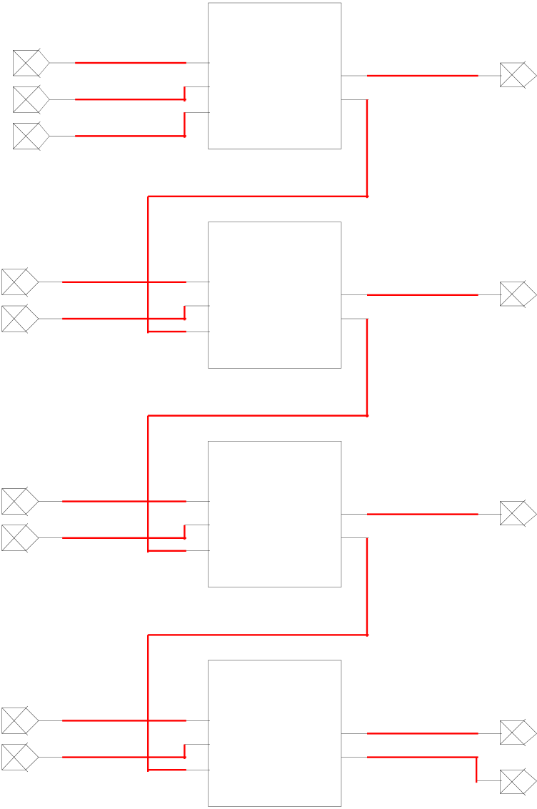
For this task, I used 4 1-bit full adders connected together. Each A and B input of the circuit corresponed to one value in the 4-bit binary number. The Cout was wired to the Cin of the next circuit and each SUM corresponded to a bit in the answer. Below is the setup for this circuit.
| A0 | A | Y0 | |
|---|---|---|---|
| B0 | B | ||
| Cin | |||
| Cin |
| A2 | A | Y2 | |
|---|---|---|---|
| B2 | B | ||
| Cin |
| A3 A2 A1 | B3 B2 B1 | Ci | Y3 Y2 Y1 | |
|---|---|---|---|---|
| A0 | B0 | n | Y0 | |
| 0 0 0 0 | 0 0 0 1 | 0 | 0 0 0 1 |
|
| 0 1 0 0 | 0 1 1 1 | 1 | 1 1 0 0 |
|
| 0 1 1 0 | 0 1 0 1 | 0 | 1 0 1 1 | |
| 1 0 1 0 | 0 0 1 1 | 1 | 1 1 1 0 | |
| 1 1 1 1 | 1 1 1 1 | 1 | 1 1 1 1 |
These tests seemed to be ground for a properly working circuit.
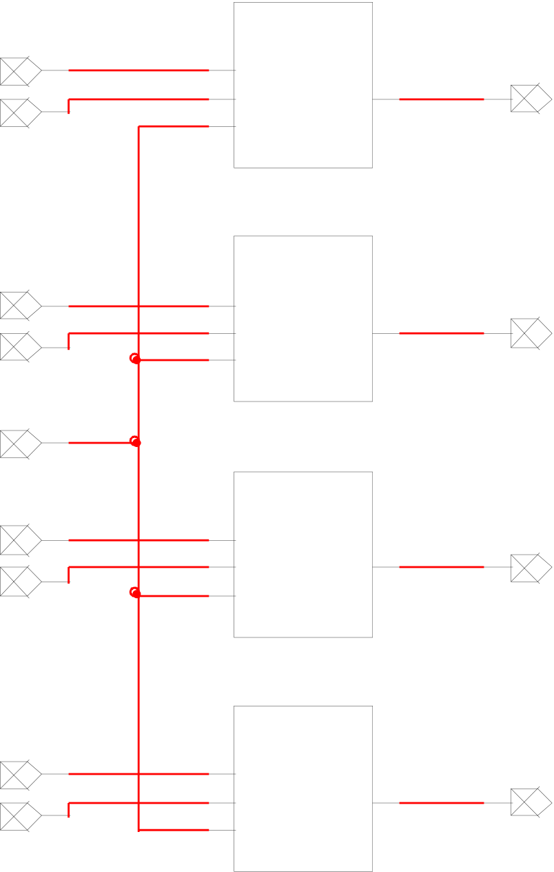
Finally, I embedded this circuit in a subcircuit for later use. Below is the subcircuit.
|
||
|---|---|---|
Task 2-4: Work Preformed
For this task, I derived an expression for the output from the truth table given in the lab report. I determined that Y = A(A/~B) + B (A/~B)’. I then proceeded to create this circuit using only the AND, OR, and NOT gates. Below is my implementation of the multiplexer.
| A/~ | A | B |
|---|
B
In the task, I was asked to build a 4-bit, 2-to-1 MUX only using the MUX created in the previous task. I was also asked to test its functionality and them embed it in a subcircuit.
| A0 | A | Y0 | |
|---|---|---|---|
| B0 | B | ||
| A/~B |
A/~B
| A2 | A | Y2 | |
|---|---|---|---|
| B | |||
| B2 | |||
| A/~B |
Figure - Circuit for 4-bit, 2-to-1 MUX
To test, the circuit, I used the following test cases.
| A3 A2 A1 | B3 B2 B1 | A/~ | |
|---|---|---|---|
| A0 | B0 | B | |
| 0 0 0 0 | 0 0 0 1 | 0 | |
| 0 0 0 0 | 0 0 0 1 | 1 |
Task 2-5: What I Learned
In this task, I learned about the functionality of the 4-bit, 2-to-1 MUX. I learned how it could be build from my 2-bit, 2-to-1 MUX that I previously built and how this could be embedded in a subcircuit for later use.Task 2-6: Build and Test a 1-to-2 Demultiplexer using AND/OR/NOT Logic
| Y/~Z | 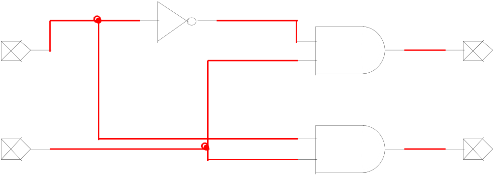 |
|
|---|---|---|
| D |
Figure - Circuit Digram of the 1-to-2 DEMUX
I then had to test the circuit using the following test cases.
| 0 | 0 | 0 | |
|---|---|---|---|
| 0 | 1 | 0 | |
| 1 | 0 | 0 |
|
| 1 | 1 | 1 |
|
Figure - Subciruit for 1-to-2 DEMUX
Task 2-8: Task Statement
In the task, I was asked to build and test a 2-to-4 decoder using only AND, OR, and NOT logic. I was also asked to embed this circuit in a subcircuit.Task 2-8: Work Preformed
For this task, I used the expression given to me in the lab manual to set up my circuit. Below is this setup.
| A1 | 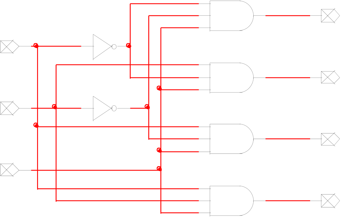 |
|
|---|---|---|
| A0 | ||
| EN | ||
Figure - Circuit Diagram of 2-to-4 Decoder
I then used the following test cases to test the functionality of the circuit.
Table - Tests for 2-to-4 Decoder
I then embedded this circuit in a sub circuit.
Figure - Subcircuit of the 1-to-2 Decoder
Task 2-8: What I Learned
In this task, I learned about the functionality of the 2-to-4 Decoder. I learned how it could be build from only AND, OR, and NOT gates and how this could be embedded in a subcircuit for later use.
| A1 | DECODER_2 | Y0 | |
|---|---|---|---|
| A1 | Y0 | ||
| A0 | A0 | Y1 | Y1 |
| Y2 | |||
| EN | Y3 | Y2 | |
Y3
| A1 | Y0 | Y8 |
|---|---|---|
| A0 | Y1 | Y9 |
| Y2 | ||
| EN | Y3 |
Y10
Y11
| A3 A2 A1 | E | |
|---|---|---|
| A0 | N |
|
| 0 0 0 1 | 0 | |
| 0 0 0 1 | 1 |
|
| 0 1 0 1 | 0 | |
| 0 1 0 1 | 1 |
DECODER_16
|
||
|---|---|---|
Figure - Subciruit for 4-to-16 Decoder
Task 2-9: What I Learned
In this task, I learned how using smaller circuits that were embedded in subciruits is the only plausible way to build large circuits.


