UK BTEC HND in Computing ECE2072 ASSIGNMENT
{`
MONASH UNIVERSITY
Department of Electrical and Computer Systems Engineering
ECE2072 ASSIGNMENT
`}
Problem Description
Design a counter that produces an output every clock cycle. The output sequence that each student downloads from Moodle contains 18 Binary Coded Decimal (BCD) digits that are unique to each student. Let’s call these output values V0, V1, V2, .. V17. The count sequence wraps around from V17 back to V0. Here is the normal count sequence:
V0 V1 V2 V3 V4 V5 …V17 V0 V1 V2 V3 V4 V5 ….
There are additional inputs with these properties:
- iSkip – when asserted the next output skips two values (eg from V0 to V3 ).
- iRev - when asserted the next output is the previous value in the sequence (eg goes from V3 to V2 ).
- When both iSkip and iRev are 1, the counter combines these effects and skips just one value (eg goes from V0 to V2 ).
- When neither iSkip nor iReverse are 1, the counter follows the normal sequence.
- iRst – when 1 the next output value is V0.
- iClk - Outputs are produced shortly after each rising Clk
Design your counter using two modules. Module CounterSkipReverse implements the state sequence of the counter in sequential logic. The module StateToCountSequence is a combinational logic circuit that maps the state to your BCD V output. Since your unique BCD V sequence necessarily contains repeated digits (there are 18 in the sequence) the BCD output cannot act as the state of the counter, as often occurs with conventional counters. The design challenge here is to work out what state representation is appropriate.
Implement your design with a minimum number of flip-flops using Verilog compiled with Quartus with the standard project settings for a DE2 board. See the assignment FAQ on Moodle for settings that may be required to ensure a minimum number of flipflops are compiled when a FSM is detected in your code by Quartus.
Question 1
Download from Moodle your Verilog template file named assignID.v that defines your count sequence V0 V1 V2 V3 V4 V5 …V17 . Note that ID in assignID.v is your 8 digit ID number. This particular file must be used for your HDL code to solve the above counter problem. Complete the modules CounterSkipReverse, StateToCountSequence and CompleteCounter. The file assignID.v must not be shared with, or shown to anyone else. Do not delete lines in this file since this may invalidate your answer during a preliminary automatic compilation, marking, plagiarism and collusion checking phase. Manual marking and checking will be used after this. Download a new copy from Moodle if you accidently delete lines.
Question 2
In your assignID.v file complete the testbench module AssignmentTestBench that enables ModelSim to check the correct functionality of your HDL design. Ensure that you test every transition from every valid state of your circuit. Since we have a reset action, we are not testing for self-starting here. Include up to four screen captures from ModelSim showing the testbench simulation with inputs, outputs and state of your design. Use appropriate display options to maximise readability.
Question 3
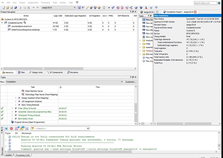
Minimise the number of Logic Cells that your design requires after a synthesis compilation in Quartus with DE2 board settings. This will involve exploring different implementation strategies, checking them with your testbench and synthesising them in Quartus. Include a screen capture of Quartus that clearly shows the number of Logic
Cells and “registers” (these are really flip-flops) after compilation for each module.
This screen capture must also show the time and date displayed on your computer. Here is an example (ignore the numbers since they are not applicable to your assignment):
Question 4
Provide a photo of a neat, clear, hand drawn sketch of a synthesised representation of your Verilog design using the following logic components only:
- Flip-flops/ registers
- Multiplexers
- AND, OR, NOT and XOR gates.
- Adders, Subtractors and Comparators (equal, less than, less than equal).
Show the signal names and the number of bits per wire that match your Verilog. See Problem Sheet 3 solution to problem 5.4 for an example. Sign and date this diagram in the bottom right corner in your own handwriting. By submitting this, you are acknowledging that this is your own work and not copied from others or shared with others.
A marking rubric will be released a week before the Moodle submission date. It will include marks allocated to the Good Style Guide below.
Good Style Guide
Follow these guidelines when writing Verilog:
- Use [N-1:0] ordering of multi-bit signals unless there is a good reason to use unconvention ordering.
- Non blocking assignments <= should be used in posedge clock always blocks. Each bit in <= assignment can synthesise a flip-flop.
- Do not mix non blocking and blocking assignments in the same always block. 4. Donot drive the same signal in two different blocks within the same module.
- Cover all input combinations for defining combinational logic from always blocks. A default assignment at the top of the block is a good way to do this.
- Think about whether don’t cares should be used in the default case statements.
- Use synchronous resets unless there is a good reason to violate timing constraints with asynchrounous resets.
- Synchronise all asynchronous inputs to the system clock with two cascaded flip-flops to allow for metastable settling as discussed in week 11 lectures.
- Use just one global clock (eg CLOCK_50) with posedge triggering in your designs. Multiple clocks and posedge with negedge triggering can cause timing problems. Clock enables (CE) can be used to select lower rate sampling than the global clock.
- Ensure you have enough bits on signals connected to an instantiation. The compiler will issue a warning message if insufficient bits are provided.
- Use named associations in port mapping for instantiations with more than 2 ports – eg Dflipflop dff1( .iClk(clk),
.iRst(rst),
.iD(data),
.oQ(out)
);
rather than rely on order:
DFlipflop dff1(clk, rst, data, out);
- Check all warning messages after compiling in Quartus and ModelSim. See 10.
- Use i and o as a prefix for port names for inputs and outputs of modules. Use _n as a suffix for asserted low or negative logic signals eg
- Use all uppercase for PARAMETER_VALUES, capitalise ModuleName and lowercase for signals.
- Avoid pointless parameters such as ONE, TWO, THREE for 1, 2, 3.
- Beware of using operators % / * (modulus divide and multiply) because they synthesise to large circuits! They are fine for test benches and simulation.
- Check your synthesised circuit after compiling. See Quartus resource usage and Quartus:Tools-> netlist viewers ->RTL viewer.
- Use an appropriate radix for readability – eg 4’d10 is the same as 4’b1010 but the former is usually more readable but this can depend on the context. Decimal is preferred unless individual bits are needed. This applies particularly to displaying signals in simulations.
- Use high level behavioural design style where possible and avoid bit level instantiation of flip-flops and hand optimised logic gates. For example a multibit counter can be defined using addition as follows always (posedge clk) count <= count + 1’b1;
rather than working with individual flip-flop instantiations and Boolean expressions for each D input.