Parallel Load Shift Register Using J-K Flip Flops
 Parallel Load Shift Register Using J-K Flip-Flops


Fig. 2 shows four flip-flops connected as a linear feedback shift register. Enter the circuit into Electronics Workbench, adding any necessary components to enable the flip-flops to be:
clocked high and low
loaded with parallel data using the pre-set and clear inputs
1. observe the Q outputs
2. Clear the registers by momentarily taking the clear inputs low.
3. Load into the register the input data ABCD = 1111, remembering that a logic ‘0’ at the pre-set input to a particular flip-flop will give a logic ‘1’ at its Q output.
4. Apply twenty clock pulses, noting your observations in the table overleaf. Comment on the sequence of numbers generated.
5. Clear the register (set all to zero) and apply three clock pulses. Comment on your results
6.
Disconnect the XOR gate input from output of gate D and connect it to the output of gate C. Repeat step 3 and comment on your observations.
| Clock Pulse | QA | QB | QC | QD | XOR connected to the outputs of FF A and D or FF A and C |
|---|---|---|---|---|---|
| 0 | 1 | 1 | 1 | 1 | |
| 1 | |||||
| 2 | |||||
| 3 | |||||
| 4 | |||||
| 5 | |||||
| 6 | |||||
| 7 | |||||
| 8 | |||||
| 9 | |||||
| 10 | |||||
| 11 | |||||
| 12 | |||||
| 13 | |||||
| 14 | |||||
| 15 | |||||
| 16 | |||||
| 17 | |||||
| 18 | |||||
| 19 | |||||
| 20 |
Universal Shift Register
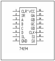
IC device- 74LS194
Simulate a shift register based on the 74LS194 Universal Shift Register IC. The pin connections and mode operation switches are shown below.
| S0 | S1 | Action |
| 1 | 1 | Parallel Load |
| 1 | 0 | Shift Right |
| 0 | 1 | Shift Left |
| 0 | 0 | Inhibit |
Serial in – Parallel out
1. Clear the register.
2. Set the parallel inputs ABCD to 0000
3. To shift right:
(a) Inhibit the Shift Left serial input by connecting it to logic ‘0’
(b) Set the mode switches for shift right operation
(c) Set the Shift Right serial input to logic ‘1’
(d) Apply four clock pulses and confirm correct operation.
4. To shift left. Proceed as 3 above, setting and inhibiting the correct inputs. Confirm correct operation.
Parallel in – Parallel out
1. Clear the register.
2. Connect the mode switches for parallel load.
3. Set ABCD to 1100 and apply one clock pulse. Note the values of the outputs.
Applying further clock pulses causes nothing to happen. Why is this?
4. Set to Shift Right and apply four clock pulses. Note the movement of data through the register.
5. Repeat the setting up procedure and demonstrate Shift Left.
Assignment Help | Sample Assignment Help | Online Assignment Help | Online Tutoring | Sample Homework